• We have updated the guidelines regarding posting political content: please see the stickied thread on Website Issues.

Nanotechnology

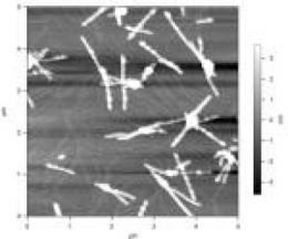
Nano-cables convert light into electricity
19:00 14 December 2006
NewScientist.com news service
Mason Inman
AdvertisementNanocables that convert light into electricity could one day be used to power nano-robots.

The cables are 16 nanometres in diameter and several micrometres long. They resemble the light-harvesting antennae used by some bacteria and transform light into electricity in a similar way to the semiconductors in solar panels, albeit on a much smaller scale.

"This is the first example of a photoconducting nanostructure," says Takanori Fukushita of the University of Tokyo, Japan, a member of the team that built the cables.

The hollow cables can grow up to several micrometres long. To build them, Fukushita and colleagues created a compound containing hexabenzocoronene (HBC), two carbon-12 chains, and trinitrofluorenone (TNF). They placed the compound in a solution of tetrahydrofuran and bubbled methane vapour though it, causing the compound to self-assemble into hollow cables.

The HBC, which sheds electrons when hit by light, formed the inside of the cable wall, and the TNF, which readily accepts electrons, coated the outside of the wall.

Light switch
Each time a photon hits the cable from outside it passes through the outer layer and knocks an electron loose from the inner layer. This causes the electron to jump to the outer layer and leave behind a positively charged "hole". These separated charges can then generate a current.

To test the nanocables, the researchers placed one on a silicon surface and applied a voltage across it. When light was shone onto the surface, a current began flowing down the cable between two electrodes. When the light was switched off, the current stopped.

At the moment, the cables cannot produce usable electricity from sunlight alone, as current does not flow well through the outer layer of TNF. The next step, Fukushita says, is to modify the outer layer, perhaps by attaching carbon-60 molecules (buckyballs), so it acts as a semiconductor and allows more current to flow.

Once this has been achieved, the nanocables could be fitted to nano-sized robots or micro-machines and power their movements, suggests Franz Würthner at the University of Würzburg in Germany. Their similarity in size and function to the antennae used by bacteria for photosynthesis means it might also be possible to connect them to such organisms, creating hybrid devices, he says.

Journal reference: Science (vol 314, p 1761)

Weblinks
Center for NanoBio Integration, University of Tokyo
http://park.itc.u-tokyo.ac.jp/CNBI/e/me ... ex_02.html
Franz Würthner, University of Würzburg
http://www-organik.chemie.uni-wuerzburg ... thner.html
Science
http://www.sciencemag.org/


www.newscientisttech.com/article/dn1079 ... city-.html
 
It is probably perfectly respectable in his own language, but Takanori Fukushita sounds kind of aggressive in English.
 
Tuesday, December 19, 2006
Making Nanoelectronics for Displays

A new way to print devices made of diverse materials could prove to be an invaluable tool in making nanoscale electronics and optics.
By Kevin Bullis
A new, inexpensive way to make nanoscale electronics could lead to, among other things, better displays, more-compact and higher-performance cell phones, and small wide-angle night-vision systems that mimic the structure of the human eye.


John Rogers, professor of chemistry and materials science and engineering at the University of Illinois, Urbana-Champaign, and his coworkers have developed a printing technique that allows them to combine a wide variety of inorganic structures, such as single-walled carbon nanotubes, assorted nanoscale wires, and ribbons made of gallium arsenide or silicon, to create multilayered, high-performance optical and electronic devices. They can also print on flexible or curved surfaces.


"This is a lovely and remarkably complete piece of work, and [it] provides probably the best method to date" for integrating dissimilar materials onto one platform, says James Heath, professor of chemistry at Caltech. It has been a challenge to do this in part because the manufacturing processes, including high-temperature deposition, that are needed for some materials can damage others. Rogers's method makes it possible to process incompatible materials separately but then combine them using a low-temperature process onto a variety of surfaces, including flexible plastic ones.


Rogers's method, which is described in the current issue of Science, begins with the fabrication of nano- and microstructures, such as an array of semiconducting silicon nanowires, using conventional techniques. The researchers then press a soft stamp onto these structures, and when the stamp is peeled away, the structures stick to it, much as dust will cling to a strip of tape. The nanostructure-bearing stamp is then pressed onto another surface that is covered with a glue-like polymer. Once this polymer cures, it adheres to the nanostructures more strongly than to the stamp: when the stamp is lifted off, it leaves the nanostructures behind, still ordered in the same configuration in which they were originally patterned. This is then repeated for the other structures.


Once the nanostructures are in place, the researchers use conventional techniques to deposit electrodes and other structures to make working devices, such as transistors. Different nanostructured materials, such as carbon nanotubes, can be printed next to the first ones on the same surface.


The method can also be used to make multilayered systems. After the first layer of devices is printed, the researchers coat it with a thin layer of the polymer glue. This serves to anchor the next layer of devices, as well as insulate between the layers. Because the polymer is thin, small holes can easily be etched into it to allow connections between selected devices in different layers.


By making it possible to easily integrate dissimilar materials onto one surface, the method could lead to smaller, more compact devices. Many electronics and optoelectronics already rely on different types of materials to perform different functions. For example, a cell phone might use high-performance gallium-arsenide semiconductors to handle high-frequency radio signals, but it might also use less-expensive conventional silicon for data processing. In the past these couldn't be easily incorporated into a single chip. One option--mounting chips side by side on a circuit board--wastes space and makes it necessary to build long, performance-degrading connections between components. In other methods, such as building up layers of wafers or depositing different materials on the same chip, the temperatures used to process some materials can limit the sorts of materials that can be combined. This can also make it impossible to place the electronics on some types of flexible surfaces, such as polymers.

The method could have an impact on various aspects of the display industry. Today's flat-screen LCD televisions are made in enormous, expensive chambers in which the electronics that control individual pixels in the display are formed on large slabs of glass. Rogers says his technique could make it possible to form these electronics in smaller batches in less expensive machines. His process could then transfer the electronics section by section to the displays to cover the glass surface. The smaller batches would also make it possible to create higher-performance silicon in these electronics, Rogers says, which would improve the response time of LCDs.


Improving LCDs is only the first step. Rogers says the technique could make it feasible to build televisions using bright and colorful light emitting diodes (LEDs) of the type used in the enormous screens at sports arenas. Because the printing method would make it easier to integrate the materials needed, the LEDs could be much smaller and more tightly packed than these large-format displays. And since the printing technique can make high-performance devices on flexible substrates, it could pave the way to roll-up LED displays.


The ability to print onto a curved surface could also make it possible to mimic the compact structure of the human eye, which could lead to smaller night-vision equipment, Rogers says.


Semprius, a University of Illinois spin-off based in Research Triangle Park, NC, has an exclusive license on the technique. Much work remains to be done to demonstrate that the device can scale up from making a handful of devices to reliably making millions for displays and night-vision systems. But Takao Someya, professor of engineering at the University of Tokyo, says that unlike past methods, which have been stymied by costs, Rogers's method offers "an ideal solution."

http://www.technologyreview.com/NanoTech/17912/
 
Tuesday, January 02, 2007
Nano Safety Alert
Concerns over the safety and environmental impact of nanomaterials mustn't be ignored.
By Seth Coe-Sullivan
Technology Review has invited members of the 2006 TR35 to tell us about their hopes for research in 2007. Seth Coe-Sullivan explains why he feels that nanotoxicity studies are critical in order for the field to thrive. Coe-Sullivan is chief technology officer of QD Vision, a Watertown, Massachusetts-based startup that is developing novel displays that use quantum dots.


Nanomaterials, and my particular obsession, quantum dots (nanocrystals that shine different colors depending on their size), are at a critical time in their development and commercialization. Decades of research have brought these materials to a stage where they can provide real value to the world; they are coming to market in a wide range of products, from wrinkle-free pants to displays for mobile devices. However, worker safety, consumer health, and the environmental impacts of such materials have to a large degree been ignored.


Some research does exist. NIOSH [National Institute of Occupational Safety and Health] has an active program for studying the safe handling of nanomaterials in the workplace. Nanotoxicity studies of carbon-based materials as well as quantum dots have been conducted, but the overwhelming conclusion is that more work is needed. All nanomaterials are not created equal and will clearly span the gamut from toxic to benign. If research helps us understand the root causes of toxicity in these materials, then safer materials can be engineered. Putting real data on toxicity into the iterative design cycle for these materials has the potential to save human lives as well as development dollars.


This year will be a critical one for setting public perception of "nano" in the United States and abroad. The EPA ruling that silver nanoparticles require separate environmental screening and classification is likely the first of many such decisions to come. Industry consortiums, environmental groups, and individual corporations need to take concrete action to determine the safety of materials and products before they are on the market. I believe that nanomaterials can be safe for consumers and the environment, but industry should recognize that the public is unlikely to give them a second chance, should we get it wrong the first time. The environment must come first, or nanomaterials will simply be asbestos writ small.


http://www.technologyreview.com/NanoTech/17954/
 
Tuesday, January 02, 2007
Remotely Activated Nanoparticles Destroy Cancer
Targeted nanotech-based treatments will enter clinical trials in 2007.
By Kevin Bullis
The first in a new generation of nanotechnology-based cancer treatments will likely begin clinical trials in 2007, and if the promise of animal trials carries through to human trials, these treatments will transform cancer therapy. By replacing surgery and conventional chemotherapy with noninvasive treatments targeted at cancerous tumors, this nanotech approach could reduce or eliminate side effects by avoiding damage to healthy tissue. It could also make it possible to destroy tumors that are inoperable or won't respond to current treatment.


One of these new approaches places gold-coated nanoparticles, called nanoshells, inside tumors and then heats them with infrared light until the cancer cells die. Because the nanoparticles also scatter light, they could be used to image tumors as well. Mauro Ferrari, a leader in the field of nanomedicine and professor of bioengineering at the University of Texas Health Science Center, says this is "very exciting" technology.


"With chemotherapy," Ferrari says, "we carpet bomb the patient, hoping to hit the lesions, the little foci of disease. To be able to shine the light only where you want this thing to heat up is a great advantage."


Although several groups are now working on similar localized treatments, Naomi Halas and Jennifer West have led the way in this area, and their work is the farthest along. (See "Nano Weapons Join the Fight Against Cancer.") Nearly ten years ago, Halas, professor of chemistry and electrical and computer engineering at Rice University, developed a precise and reliable method for making nanoshells, which can be hollow spheres of gold or, in the case of the cancer treatment, gold-coated glass spheres. These spheres are small enough (about 100 nanometers in diameter) to slip through gaps in blood vessels that feed tumors. So as they circulate in the bloodstream, they gradually accumulate at tumor sites.


Halas tuned the nanoparticles to absorb specific wavelengths of light by changing the thickness of the glass and gold. For the cancer treatment, she selected infrared wavelengths that pass easily through biological tissues without causing damage. To destroy a nanoshell-infiltrated tumor, the tumor is illuminated with a laser, either through the skin or via an optical fiber for areas such as the lungs.


"We shine light through the skin, and in just a few minutes, the tumor is heated up," Halas says. "In the studies that were initially reported--and this has been repeated now more than 20 times in at least three different animal models--we have seen essentially 100 percent tumor remission." The tests also suggest the nanoshells are nontoxic. Halas says they are eliminated from the body through the liver over several weeks. The technology was developed at Rice in collaboration with Jennifer West, a professor of bioengineering. It has been licensed by Nanospectra Biosciences, a startup based in Houston, TX, that is beginning the process of getting FDA approval for clinical trials for treating head and neck cancer. In the future, the technology could be used for a wide variety of cancers.


"There is a potential for this to bring a profound change in cancer treatment," Halas says. "For the case of someone discovering a lump in their breast, this would mean that a very simple procedure could be performed that would induce remission." She says that "for many, many cases of cancer, rather than the lengthy chemotherapy or radiation therapy," an individual would have "one simple treatment and very little side effects."


Halas anticipates that approval for the method will come quickly, in part because the nanotechnology is not a drug but a device, for which the approval process is simpler. Also, she expects it will perform the same in humans as in animal models, "because heat and light work in exactly the same way whether you're in a pig, a dog, [or] a human being."


Since their initial experiments, the researchers have been further developing the technology. They've demonstrated the ability to coat the nanoshells with antibodies that latch on to breast-cancer cells, further improving the selectivity of the treatment. They've also attached molecules that make the nanoshells into pH sensors that would be useful for both imaging tumors and as an "optical biopsy" for identifying cancers, Halas says.


The clinical trials this year will not take advantage of these advances. But eventually the antibody targeting could make preventative cancer treatments possible. "If you have the genetic profile for prostate cancer occurring in your family, one could imagine treating extremely early stages, when you have something a millimeter or smaller which you could barely visualize," Halas says. "With antibody targeting and then illumination of that region, you could destroy those cells at a very early stage. You could have a treatment every five to ten years, and then you would be free of the disease." The nanotechnology could also be used to eradicate cancers that have spread too much to be removed by surgery.


While people will not be able to take advantage of these advances in the near future, Halas says that treatments based on the original design could be available in a couple of years. Ferrari cautions that most treatments do not make it through clinical trials, but, he says, "I'm hopeful that their clinical trials will yield great results."

http://www.technologyreview.com/NanoTech/17956/
 
Hybrid Structures Combine Strengths of Carbon Nanotubes and Nanowires

A team of researchers at Rensselaer Polytechnic Institute has created hybrid structures that combine the best properties of carbon nanotubes and metal nanowires. The new structures, which are described in a recent issue of Applied Physics Letters, could help overcome some of the key hurdles to using carbon nanotubes in computer chips, displays, sensors, and many other electronic devices.

The impressive conductivity of carbon nanotubes makes them promising materials for a wide variety of electronic applications, but techniques to attach individual nanotubes to metal contacts have proven challenging. The new approach allows the precise attachment of carbon nanotubes to individual metal pins, offering a practical solution to the problem of using carbon nanotubes as interconnects and devices in computer chips.


“This technique allows us to bridge different pieces of the nanoelectronics puzzle, taking us a step closer to the realization of nanotube-based electronics,” said Fung Suong Ou, the paper’s corresponding author and a graduate student in materials science and electrical engineering at Rensselaer.

As chip designers seek to continually increase computing power, they are looking to shrink the dimensions of chip components to the nanometer scale, or about 1-100 billionths of a meter. Carbon nanotubes and nanowires that became available in the 1990s are promising candidates to act as connections at this scale, according to Ou, because they both possess interesting properties.

For example, carbon nanotubes display amazing mechanical strength, and they are excellent conductors of electricity, with the capacity to produce interconnects that are many times faster than current interconnects based on copper. Gold nanowires also have very interesting optical and electrical properties, and they are compatible with biological applications, Ou said.

“In order to take full advantage of these materials, we demonstrate the idea of combining them to make the next generation of hybrid nanomaterials,” he said. “This approach is a good method to marry the strengths of the two materials.”

The metal nanowires in this technique are made using an alumina template that can be designed to have pore sizes in the nanometer range. Copper or gold wires are deposited inside the pores, and then the entire assembly is placed in a furnace, where a carbon-rich compound is present. When the furnace is heated to high temperatures, the carbon atoms arrange themselves along the channel wall of the template and the carbon nanotubes grow directly on top of the copper wires.

“It’s a really easy technique, and it could be applied to a lot of other materials,” Ou said. “The most exciting aspect is that it allows you to manipulate and control the junctions between nanotubes and nanowires over several hundred microns of length. The alumina templates are already mass-produced for use in the filter industry, and the technique can be easily scaled up for industrial use.”

To date the team has made hybrid nanowires that combine carbon nanotubes with both copper and gold. But they also are currently working to connect carbon nanotubes to a semiconductor material, which could be used as a diode, according to Ou.

The research was performed under the guidance of Pulickel Ajayan, the Henry Burlage Professor of Materials Science and Engineering at Rensselaer and a world-renowned expert in fabricating nanotube-based materials. Other Rensselaer researchers involved with the project were Robert Vajtai, Derek Benicewicz, Lijie Ci, and M.M. Shaijumon.

Source: Rensselaer Polytechnic Institute


http://www.physorg.com/news87471930.html
 
Homing Nanoparticles Pack Multiple Assault On Tumors
Main Category: Cancer / Oncology News
Article Date: 10 Jan 2007 - 22:00 PST
| email this article | printer friendly | view or write opinions | Article Also Appears In
Blood / Hematology


Useful Article?
Digg It
Del.icio.us
NewsVine
Reddit


A collaborative team led by Erkki Ruoslahti, M.D., Ph.D., of the Burnham Institute for Medical Research at UC Santa Barbara (Burnham) has developed nanoparticles that seek out tumors and bind to their blood vessels, and then attract more nanoparticles to the tumor target. Using this system the team demonstrated that the homing nanoparticle could be used to deliver a "payload" of an imaging compound, and in the process act as a clotting agent, obstructing as much as 20% of the tumor blood vessels. These findings are pending publication in the Proceedings of the National Academy of Sciences and will be made available at the journal's website during the week of January 8, 2007.

The promise of nanomedicine is based on the fact that a particle can perform more functions than a drug. Multifuncionality is demonstrated in the current study, in which researchers from Burnham, UC San Diego, and Massachusetts Institute of Technology designed a nanoparticle that combined tumor-homing, self-amplification of the homing, obstructing tumor blood flow, and imaging.

Using a screening technique developed previously in Ruoslahti's laboratory, the group identified a peptide that homed to the blood vessels, or vasculature, inside breast cancer tumors growing in mice. The peptide was comprised of five amino acids: Cysteine-Arginine-Glutamic acid-Lysine-Alanine, abbreviated CREKA.

The researchers then demonstrated that the CREKA peptide recognizes clotted blood, which is present in the lining of tumor vessels but not in vessels of normal tissues. They used a special mouse strain that lacks fibrinogen, the main protein component of blood clots, to show this: tumors growing in these fibrinogen-deficient mice did not attract the CREKA peptide, whereas the peptide was detected in the tumors of a control group of normal littermates.

Having confirmed clotted blood as the binding site for CREKA, the team constructed nanoparticles from superparamagnetic amino dextran-coated iron oxide (SPIO); such particles are used in the clinic to enhance MRI imaging. They coupled the CREKA peptide to the SPIO particles to give the particles a tumor-homing function and programmed an additional enhanced imaging functionality into their nanoparticle by making it fluorescent.

Initially, CREKA-SPIO's tumor homing ability was impeded by a natural defense response, which activates the reticuloendothelial system (RES)--white blood cells which together with the liver and spleen comprise a protective screening network in mice (and humans). The investigators devised "decoy" molecules of liposomes coated with nickel, which diverted the RES response that would have otherwise been directed toward CREKA-SPIO. The use of decoy molecules extended the half-life of CREKA-SPIO in circulating blood five-fold, which greatly increased the nanoparticle's ability to home to tumors.

The CREKA-SPIO that accumulated in the tumor enhanced blood clotting in tumor vessels, creating additional binding sites for the nanoparticles. This "self amplification" of the tumor homing greatly enhanced the investigators' ability to image the tumors. It also contributed to blocking as much as 20% of the blood vessels in the tumor. While occluding 20% of tumor vessels was not sufficient to reduce the rate of tumor growth, it is a promising target for future studies.

"Having identified the principle of self-amplification, we are now optimizing the process, hoping to obtain a more complete shut-down of blood flow into the tumor to strangle it," says Ruoslahti. "We are also in the process of adding a drug delivery function to the particles. These two approaches are synergistic; the more particles we bring into the tumor, the greater the obstruction of the blood flow and more of the drug is delivered into the tumor."

###

Co-authors on this publication include: Dimitri Simberg, Tasmia Duza, Markus Essler, Jan Pilch, Lianglin Zhang, Austin Derfus, contributing from Dr. Erkki Ruoslahti's laboratories at Burnham Institute for Medical Research and Burnham Institute for Medical Research at UC Santa Barbara; Michael Sailor, Ji Ho Park, Austin Derfus, and Robert Hoffman, from University of California, San Diego; Sangeeta Bhatia, from Massachusetts Institute of Technology; and Meng Yang and Robert Hoffman from AntiCancer, Inc., San Diego, California.

This work was supported with funding from the National Institutes of Health.

Dr. Erkki Ruoslahti is Distinguished Professor and former President and CEO at Burnham. He recently founded the "Vascular Mapping Center" at Burnham-UC Santa Barbara, which aims at developing applications for vascular "zip codes, molecular signatures in blood and lymphatic vessels ("vasculature") that are specific to individual tissues and disease sites.

Burnham-UCSB, was established in 2006 through a collaborative effort of the Burnham Institute for Medical Research, based in La Jolla, California, and the University of California at Santa Barbara.

Burnham Institute for Medical Research is an independent non-profit research institution dedicated to advancing the frontiers of scientific knowledge in the life sciences and medicine, and providing the foundation for tomorrow's innovative therapies. The Institute is home to three major centers: the National Cancer Institute-designated Cancer Center, the Del E. Webb Center for Neuroscience and Aging Research, and the Infectious and Inflammatory Disease Center. Established in 1976 in La Jolla, California, Burnham today employs over 750 people and ranks consistently among the world's top 20 research institutes in independent surveys conducted by the Institute for Scientific Information. Burnham recently announced plans to open a campus in Orlando, Florida that will extend the Institute's capabilities in drug discovery and genomics, as well as expand its research to cover more types of diseases. For additional information about Burnham and to learn about ways to support its research, visit http://www.burnham.org/.

Contact: Nancy Beddingfield
Burnham Institute

http://www.medicalnewstoday.com/medical ... wsid=60429
 
Nanotechnology In China: Ambitions And Realities
Main Category: Conferences News
Article Date: 15 Jan 2007 - 6:00 PST


A senior Department of Commerce official recently claimed that China is rapidly catching up to the United States in nanotechnology. This news comes on top of the latest OECD (Organization for Economic Co-operation and Development) forecast that China will have spent more on research and development (R&D) than Japan in 2006, making it the world's second highest investor in R&D after the U.S.

Nanotechnology--the manipulation of materials at very small sizes, where these materials take on novel or unusual physical and chemical properties--is a field of intense international competition. Some experts predict nanotechnology will be as important as the steam engine, the transistor, and the Internet. Worldwide, governments and corporations invested almost $10 billion in nanotechnology R&D in 2005.

Is China poised to become the world's nanotech superpower, or is this prediction hyperbole? What is China's comparative advantage in the high-tech sector, and how is it exploiting this advantage in nanotechnology? Will China's investment in nanotechnology pay off? And how will the United States respond to China's growing nanotechnology capacity--with competition, cooperation, or both?

These questions are the topic of an event and live webcast on Tuesday, February 6th at 3:00 p.m. in the 5th Floor Conference Room of the Woodrow Wilson International Center for Scholars (http://mailto:www.wilsoncenter.org/directions).

*** Webcast LIVE at http://www.wilsoncenter.org/***

What: Nanotechnology in China: Ambitions & Realities

Who: Dr. Denis Fred Simon, Provost and Vice President for Academic Affairs, Levin Institute, State University of New York

Dr. Richard P. Appelbaum, Executive Committee, Center for Nanotechnology in Society and Professor, Sociology and Global & International Studies, University of California at Santa Barbara Evan Michelson, Research Associate, Woodrow Wilson Center's Project on Emerging Nanotechnologies, Moderator

When: Tuesday, February 6th, 2007, 3:00 - 4:00 p.m.

Where: Woodrow Wilson International Center for Scholars, 5th Floor Conference, Room. 1300 Pennsylvania Avenue, NW, Washington, DC 20004

This event is organized by the following programs at the Wilson Center: Project on Emerging Nanotechnologies, Asia Program, China Environment Forum, and the Program on Science, Technology, America & the Global Economy.

###

The Project on Emerging Nanotechnologies was launched in 2005 by the Wilson Center and The Pew Charitable Trusts. It is dedicated to helping business, governments, and the public anticipate and manage the possible health and environmental implications of nanotechnology.

Contact: Julia Moore
Project on Emerging Nanotechnologies

http://www.nanotechproject.org/


http://www.medicalnewstoday.com/medical ... wsid=60566
 
Chemists Make Molecular Rings in Shape of King Solomon's Knot


chemistsmake.jpg


Mosaic image of King Solomon’s knot. UCLA chemists have made, at the nanoscale, molecular interlocked rings in the shape of the knot, a symbol of wisdom. Credit: UCLA

UCLA chemists have made, at the nanoscale, a molecular compound of interlocked rings that has the shape of the ancient King Solomon's knot, a symbol of wisdom that is thousands of years old and is widely used in architecture and works of art. The Bible portrays Solomon as great in wisdom, wealth and power.

"King Solomon, according to Italian legend, was on a hill and was charged by God with protecting a village from large boulders that were going to roll down and destroy the village," said UCLA chemistry graduate student Cari Pentecost, lead author of the Solomon's knot research, which was published in this year's first issue of the German chemistry journal Angewandte Chemie. "King Solomon was holding three large boulders and took a rope and devised this knot to support the boulders and protect the town."

"Our research is a marriage of nanoscience, mathematics and art," Pentecost added.

The Solomon's knot is composed of two rings that interlace each other four times, with alternating crossing points that go over, under, over and under as one traces around each of the rings. Pentecost's nano-version is roughly 2 nanometers high - about 1,000 times smaller than a red blood cell and 10,000 times smaller than the diameter of a human hair - by 1.2 nanometers wide.

Pentecost conducts research in the laboratory of J. Fraser Stoddart, director of the California NanoSystems Institute (CNSI), who holds UCLA's Fred Kavli Chair in Nanosystems Sciences and who last December was awarded a knighthood by Queen Elizabeth II of Britain for his work in chemistry and nanotechnology.

Pentecost produced the molecular Solomon's knot while performing experiments on molecular Borromean rings, which are comprised of three interlocked rings that form an inseparable union such that cutting any one ring results in the other two falling apart. Stoddart's research team developed this mechanically interlocked Borromean compound in 2004, and the research was published in the May 28, 2004, issue of Science.

Pentecost decided to change the recipe for making molecular Borromean rings ever so slightly. With the knowledge that if she used either zinc or copper ions as the template for a particular chemical reaction, she would get only the molecular Borromean rings, Pentecost instead used equal amounts of zinc and copper ions, and the result was crystals of the molecular Solomon's knot 10 out of 10 times.

"Synthetic chemistry is ready to make substantial inroads into some quite exotic molecules in the shape of knots and links," said Stoddart, who believes the molecular Borromean rings and the Solomon's knot are likely to have future applications. "There is oftentimes a connection between the beauty and elegance of a chemical structure and its potential usefulness, and this Solomon knot structure is quite beautiful and elegant."

The Solomon's knot is carved, painted, sculpted, stitched, crocheted, knitted, inlaid and beaded in cultural relics from Europe, the Middle East and elsewhere, according to Lois Rose Rose, author of "Seeing Solomon's Knot" and a UCLA graduate. The design, which is found in numerous buildings, can be seen in the floor tiles and on the wooden ceilings of UCLA's Powell Library and on the outside architecture of UCLA's Haines Hall and Moore Hall.

"Here I am, making molecules of these Solomon's knots, and everywhere I go on the campus, they are staring me in the face or I am walking into them," Pentecost said.

Speaking of the excitement of nanoscience, Stoddart said, "We have to try to rediscover the spirit of the Renaissance, when there were no boundaries. Nanoscience is a replay of previous industrial revolutions. In the 21st century, people will start to appreciate what a nanoparticle or nanowire is, just as in the past they embraced the invention of the wheel or the highway."

Stoddart said that making the molecular counterparts of Borromean rings and Solomon's knots is a form of chemical evolution on the nanoscale.

"In the making of these exotic compounds, chemical bonds are being broken just as fast as they are being formed, until the compound that feels most comfortable emerges as the final product," he said. "A kind of Darwinian selection process is going on in a playful kind of way in the 'room at the top.' Cari Pentecost's contribution was to find, accidentally, the particular set of keys that opens the combination lock to the door to yet another of these rooms at the top."

Co-authors on the research are former UCLA postdoctoral scholars Kelly Chichak and Andrea Peters, both of whom worked in Stoddart's research group; Gareth Cave, an X-ray crystallographer at Nottingham Trent University; and Stuart Cantrill, a former research associate in Stoddart's research group.

Source: UCLA

http://www.physorg.com/printnews.php?newsid=87669806
 
Nanotechnology shows promise as next wrinkle fighter

The next big idea in preventing wrinkles is very, very small. Nano small.

A Michigan State University chemical engineer has discovered that nanoparticles can stop thin polymer films from buckling and wrinkling. It's a new solution to a critical problem as thin films become more important in new technology such as electronic monitors.

The cosmetic arsenal to fight human wrinkles embraces technologies that seems crossed with science fiction – from microdermabrasians to lasers to Botox injections – and nanoparticles are poised to join the war by warding off dreaded buckles in human skin.

Ilsoon Lee, an assistant professor of chemical engineering, along with Ph.D. student Troy Hendricks, published an online article in the American Chemical Society's Nano Letters in December 2006 that outlines the potential of using infinitesimally small nanoparticles – 50nm – between films to smooth out the tiny buckles that are the origin of wrinkles.

While the article addresses breakthroughs in the buckling of polymer films as they were compressed or heated during the manufacturing process, Ilsoon said the principles show promise to apply to human skin.

The research is supported by the National Science Foundation and the Michigan Economic Development Corp.

On all fronts, it's all about nailing a wrinkle before it starts.

"Everything starts at a really small scale, so if we can prevent the buckling at the very beginning – at the nano level – we can eliminate large scale wrinkles," Ilsoon said. "Wrinkles can initiate from the small scale, and when it grows we cannot remove it."

Nanoparticles already have entered the cosmetic marketplace because they can penetrate deeper into the skin, transporting vitamins and other compounds to plump and smooth tissue. But Ilsoon envisions thin films that can be injected beneath the thinning outer layer of the skin, the epidermis, that over time stiffens and buckles with aging, and the thicker dermis beneath it, which remains more pliable over time. Think of a raisin.

Ilsoon explained that nanoparticles spread in a thin film can break up the compressive forces on a plane and redirect them. Once the force is reduced below the critical buckling strain, the film will not
buckle. No buckles, no wrinkles. The nanoparticles in the film can be stress busters without affecting the neighboring layers.

"The wrinkle-free films will automatically absorb or deflect the stress and stay flat, just as they are after formation," he said.

Nanoparticle films wouldn't be a face-lift itself, but Ilsoon sees the possibility in a film that could be added during a cosmetic procedure – such as an eyelift – to stabilize the improvements and prevent further wrinkling. He also sees applications in medical procedures – such as artificial skins for surgery.

The ideas are in the early stages with health and safety concerns to be worked through. Already Ilsoon's lab, with collaborators, is testing polymer films, by applying various cells and proteins to see if there are toxic reactions.

Source: Michigan State University


http://www.physorg.com/printnews.php?newsid=88188834
 
Delft Nano-Detector Very Promising For Remote Cosmic Realms

The hot-electron bolometer (logarithmic-spiral antenna is the circular area in the center) is formed on a silicon chip which is glued to a hyper-hemispheric lens.
by Staff Writers
Delft, Holland (SPX) Jan 18, 2007
A miniscule but super-sensitive sensor can help solve the mysteries of outer space. Cosmic radiation, which contains the terahertz frequencies that the sensors detect, offers astronomers important new information about the birth of star systems and planets.
Merlijn Hajenius developed these sensors for Delft University of Technology's Kavli Institute of Nanoscience, in close cooperation with the SRON Netherlands Institute for Space Research. He will receive his Delft University of Technology PhD degree on 19 January based on this research subject.

The detector, called a 'hot electron bolometer', is based on the well-known phenomenon that electrical resistance increases when something is heated up. The use of a superconductor renders the detector extremely sensitive and allows it to be used for radiation that until now could not be so well detected.

The detector works for terahertz frequencies, which astronomers and atmospheric scientists are extremely interested in. The detector's core is comprised of a small piece of superconducting niobiumnitride. Clean superconducting contacts that are kept at a constant temperature of -268 C (five degrees above absolute zero) are attached to both ends of the superconducting niobiumnitride.

A miniscule gold antenna catches the terahertz-radiation and sends it via the contacts to the small piece of niobiumnitride, which functions as an extremely sensitive thermometer. "By reading this thermometer, we can very accurately measure the terahertz radiation. In Delft, we have set a world record with this detector in the frequency area above 1.5 terahertz," Hajenius says proudly.

The results have convinced astronomers to use these detectors for the new observatory in Antarctica (HEAT), and a new space mission (ESPRIT) has also been proposed.

The 'maiden flight' of Hajenius' detector is planned for next year, but it will not take place in a satellite used for studying cosmic clouds, but rather in a balloon that will study the earth's atmosphere. The TELIS instrument, which SRON is currently working on, will be equipped with a Delft University of Technology detector and will measure the molecules in the atmosphere above Brazil that influence the formation of the hole in the ozone layer.


Nano
 
Nanopolymers make their debut
19 January 2007

Researchers in the US have made a new class of materials called "nanopolymers" -- the first nanoscale equivalents of polymers. The breakthrough was made by Francesco Stellacci and colleagues at the Massachusetts Institute of Technology and involves introducing defects onto two opposing areas on the surface of spherical-shaped metallic nanoparticles. The resulting divalent particles are then chained together to make freestanding films (Science 315 358).


Figure 1
Nanoparticles are nanometre-sized collections of atoms that can be used as building blocks to make a wide variety of materials, such as supercrystals or ionic liquids. However, they lack the ability to bond along specific directions -- like atoms and molecules do -- which means they are not easily joined together to make large structures like filaments or films. This is because nanoparticles are typically coated with a capping layer to prevent further growth or clustering.


Figure 2
Now, Stellacci and colleagues have found a way to overcome this problem. The researchers effectively break the symmetry of the round nanoparticles by bonding two different types of ligand, such as thiol molecules, onto the poles of the spheres. The ligands on one nanoparticle are then free to bond with the ligands on the other particles so they can then be chained together to form the nanoscale equivalent of polymers (figures 1 & 2). The chaining reaction, which takes just a few hours, is very similar to way nylon polymerizes to form chains, says Stellacci.


Figure 3
The scientists confirmed their result by taking tunnelling electron microscope images of the nanoparticle chains. The number of nanoparticles in each chain varies widely but the maximum number counted was 50,000 nanoparticles molecularly linked together (figure 3). Some chains even produced a continuous film as large as a square centimetre across and 60 µm thick.

"The main application of this work is in the generation of a new class of materials called nanopolymers with substantially novel properties, such as controlled porosity on the nanoscale," said Stellacci. "These polymers will allow fundamental investigations of material properties – for example, can such materials retain glass transition temperatures and if so, how viscous is the glass?"

The team now plans to make longer chains of nanoparticles.

About the author
Belle Dumé is acting editor on nanotechweb.org

http://physicsweb.org/articles/news/11/1/17/1
 
Nano-wheels seen rolling at last
12:18 22 January 2007
NewScientist.com news service
Tom Simonite
AdvertisementIt is the nano-equivalent of seeing the first stone disc roll down a prehistoric hill: German and French scientists have, for the first time, observed a nanoscopic wheel rolling over a flat surface.

The researchers created a carbon molecule resembling a pair of wheels just 0.8 nanometres in diameter, joined together by an axle only four carbon atoms long. The achievement was a combined effort by researchers at the Free University of Berlin in Germany and the Center for Material Elaboration & Structural Studies in Toulouse, France.

After being chemically synthesised in the lab, hundreds of these "nanowheels" were sprayed onto a sheet of copper. The researchers then used the tip of a scanning tunnelling electron microscope (STEM) to push individual molecules across a copper surface.

Right direction
"Using the STEM provided a direct readout that shows the wheels [only] roll when pushed in the right direction," perpendicular to the axle, says Leonhard Grill, leader of the German research team, told New Scientist. If nudged the wrong way, the molecules instead skip across the surface.

The tip of the microscope is so sharp, its point is just a single atom wide. This is connected to an electric circuit linked to a substrate that supports a sample. Electrons "tunnel" from the tip to the sample to the substrate beneath and subtle variations in current reveal features of the sample.

The microscope confirmed that the nanowheels will only roll in the correct direction. "When we pushed in a direction that doesn't allow the wheel to rotate we got a different pattern that shows they hop across the surface," says Grill.

Rolling readout
Grill acknowledges that other researchers have previously made nanoscale wheels. "They have done good research," he says. "The only thing that was missing was a direct readout of rolling."

One such team is led by James Tour at Rice University in Houston, US (see Nano-car gets an engine). "We say that our wheels are rolling based on the fact that the 'cars' moved forward and back, and never side to side," Tour explains.

"It's fascinating to reproduce movement so important in our world at this scale," adds Grill. Because wheels can only travel in certain directions, they could provide a useful tool for nanoscale manufacturing he suggests: "Any nano-device made from different parts needs to be assembled; rolling could be one way of doing that."

Journal reference: Nature Nanotechnology (DOI: 10.1038/nnano.2006.210)

Related Articles
Nanotube coating promises ice-free windscreens
http://www.newscientisttechnology.com/article/dn10850
21 December 2006
Nano-welds herald new era of electronics
http://www.newscientisttechnology.com/article/dn10824
19 December 2006
Nano-car gets an engine
http://www.newscientisttechnology.com/article/dn9004
14 April 2006
Weblinks
Nanoscience with Functionalized Molecules, Free University of Berlin
http://www.physik.fu-berlin.de/~grill/
Center for Material Elaboration and Structural Studies, Toulouse
http://www.cemes.fr/r7_english/index.htm
James Tour's research group, Rice University, Houston
http://www.jmtour.com/


www.newscientisttech.com/article/dn1100 ... -last.html
 
Nano World Off The Radar For Most
24 Jan 2007

Sunscreens contain nano particles, carbon and titania nanotubes show promise and nano structures are the rage in engineering schools. While the proliferation of nano research may signal a mini revolution, outside the realms of business and science, this insurgency may be no more than a whisper, according to an international team of researchers.

"In the last 15 years we have continuously been exposed to a variety of emerging technologies - biotechnology, information science and technology, cognitive science and now nanotechnology," says Dr. Akhlesh Lakhtakia, the Charles Godfrey Binder Professor of Engineering Science and Mechanics at Penn State. "Education is the key to understanding these areas."

However, when it comes to nanotechnology, Lakhtakia and his colleagues found that people in most segments of the economy are not paying much attention. Or, if they are aware of the field, the reactions and actions are overly enthusiastic, uninformed or alarmist.

Lakhtakia, working with Debashish Munshi, associate professor, management communications and Priya Kurian, senior lecturer, political science and public policy, University of Waikato, New Zealand, and Robert V. Bartlett, the Gund Professor of Liberal Arts, University of Vermont, looked at how technologists/scientists, business and industry leaders, government agencies, social science researchers, fiction writers, political activists, science journalists and writers and the general public view nanotechnology.

Scientists have, of course, picked up on nanotechnology. The word proliferates through the literature and is prominent in proposals for funding. In an article in the international journal Futures, published by Elsevier, tresearchers note that "entrepreneurial technoscientists have learned to align their research efforts with the latest terms in vogue." However, it is not always clear what that nanotechnology means.

"Carbon nanotubes, quantum dots, sculptured thin films, single-electron transistors, nanofluidic sensors and biomimetic substances are all examples of evolutionary nanotechnology," says Lakhtakia. "None has yet had any significant presence in the marketplace and these developments will not be real for many years."

Currently, normal incremental changes bring sizes down to 100 nanometers - and, therefore, qualify research as nanoscience. However, simply making particles smaller for cosmetics or reinforcing plastics with carbon nanofibers is not breakthrough science, although these advances are turning out to be lucrative.

Business leaders view nanotechnology with cautious optimism. Most investment aims to improve existing products by creating smaller components or smaller products with less interest in new materials or products. Investors are wary of a nanotechnology boom turning into a dot.com-like bust.

Government and quasi-official organizations find nanotechnology important. The U.S. established an Interagency Working Group on Nanotechnology in 1996 and in 2000 the National Nanotechnology Initiative began coordinating efforts in nanotechnology. The National Science Foundation conducted a workshop on the societal impacts of nanotechnology in 2000 and concluded that, while there were technological and economic benefits to come, the societal impacts down the road were unknown. They recommended including social scientists in the NNI.

Among social scientists, little work on nanotechnology exists. While some have begun to study the area, there is little published. Reports from government agencies, scientists and business interests form the basis of the little that does exist. Some social scientists find nanotechnology interesting and beneficial, but others equate nanotech with areas they found frightening such as genetic engineering or cloning. Currently no nanotechnology law exists and legal experts believe that current law is sufficient to handle future needs with modification.

Fiction writers have covered nanotechnology, both good and bad, for a long time. Novels like Crichton's "Prey" emphasize the negatives of nanotechnology, while others expand on the possibilities. These writers reflect the hopes and fears of the scientific community and feed the nascent research of the social scientists. A Canadian activist group produced a series of reports on the social implications of nanotechnology and urges caution in using nanotechnology. Greenpeace called for a moratorium on nanotechnology due to potential nanoparticle toxicity. Many anti-nanotechnology activists predict the creation of destructive, uncontrollable life forms from nanotechnology. However, some activists realize the potential good and suggest caution as the best approach to development.

Science writers and journalists report the scientific research as it comes into the literature. They also cover the reports evaluating nanotechnology, such as the Canadian reports on social implications. Science writers have not yet produced broad evaluations of the field, but have begun to evaluate the business aspects in the cautionary context of a dot.com bust.

"The paucity of debate and critical analysis on the implications of nanotechnology in the popular media is reflected in the general lack of public awareness of the implications of nanotechnology," according to the researchers.

The researchers find the general public only vaguely aware of nanotechnology. The public sees nanotechnology as having some benefits, but is concerned with how business and industry develop the field. In the U.S., the idea of science as a neutral endeavor creates a view of nanotechnology as good, providing untold opportunities. However, the majority is unaware of exactly what nanotechnology is and of the potential problems in its development.

"Schools must find a way to interweave science, engineering, liberal arts, literature and history so that emerging fields like nanotechnology, biotechnology and cognitive science can be understood and evaluated by the general public," Lakhtakia of Penn State says. "Lifelong learning is also necessary to keep up with the changes as they come along." ###

Contact: A'ndrea Elyse Messer
Penn State http://live.psu.edu/


http://www.medicalnewstoday.com/medical ... wsid=61394
 
Coated nanoparticles solve sticky drug-delivery problem

The layers of mucus that protect sensitive tissue throughout the body have an undesirable side effect: they can also keep helpful medications away. To overcome this hurdle, Johns Hopkins researchers have found a way to coat nanoparticles with a chemical that helps them slip through this sticky barrier.

During experiments with these coated particles, the researchers also discovered that mucus layers have much larger pores than previously thought, providing a doorway that should allow larger and longer-acting doses of medicine to reach the protected tissue.

The team's findings were reported this week in the Early Online Edition of Proceedings of the National Academy of Sciences.

The discoveries are important because mucus layers, which trap and help remove pathogens and other foreign materials, can block the localized delivery of drugs to many parts of the body, including the lungs, eyes, digestive tract and female reproductive system. Because of these barriers, doctors often must prescribe pills or injections that send drugs through the entire body, an approach that can lead to unwanted side effects or doses that are too weak to provide effective treatment.

"Mucus barriers evolved to serve a helpful purpose: to keep things out," said Justin Hanes, an associate professor of chemical and biomolecular engineering who supervised the research. "But if you want to deliver medicine in a microscopic particle, they can also keep the drugs from getting through. We've found a way to keep helpful nanoparticles from sticking to mucus, and we learned that the openings in the mucus 'mesh' are much larger than most people expected. These findings set the stage for a new generation of nanomedicines that can be delivered directly to the affected areas."

To get its particles past the mucus, Hanes' team studied an unlikely model: viruses. Earlier research led by Richard Cone, a professor in the Department of Biophysics at Johns Hopkins, had established that some viruses are able to make their way through the human mucus barrier. Hanes and his colleagues decided to look for a chemical coating that might mimic the characteristics of a virus.

"We found that the viruses that got through had surfaces that were attracted to water, and they had a net neutral electrical charge," said Samuel K. Lai, a Johns Hopkins chemical and biomolecular engineering doctoral student from Canada and Hong Kong who was lead author of the journal article. "We thought that if we could coat a drug-delivery nanoparticle with a chemical that had these characteristics, it might not get stuck in the mucus barrier."

To make their nanoparticles behave like viruses, the researchers coated them with polyethylene glycol, PEG, a non-toxic material commonly used in pharmaceuticals. PEG dissolves in water and is excreted harmlessly by the kidneys.

The researchers also considered the size of their nanoparticles. Previous studies indicated that even if nanoparticles did not stick to the mucus, they might have to be smaller than 55 nanometers wide to pass through the tiny openings in the human mucus mesh. (A human hair is roughly 80,000 nanometers wide.) Using high-resolution video microscopy and computer software, the researchers discovered that their PEG-coated 200-nanometer particles could slip through a barrier of human mucus.

They then conducted further tests to see how large their microscopic drug carriers could be before they got trapped in the mesh. Larger nanoparticles are more desirable because they can release greater amounts of medicine over a longer period of time. "We wanted to make the particles as large as possible," said Hanes, who also serves as director of therapeutics for the Institute for NanoBioTechnology at Johns Hopkins. "The shocking thing was how fast the particles that were 500 nanometers wide moved through the mucus mesh. The work suggests that the openings in the mucus barrier are much larger than originally expected by most. And we were also surprised to find that the larger nanoparticles (200 and 500 nanometers wide) actually moved through the mucus layer more quickly than the smaller ones (100 nanometers wide)."

This has important implications, Hanes said, because a 500-nanometer particle can be used to deliver medicine to a targeted area, released over periods of days to weeks. Larger particles also allow a wider array of drug molecules to be efficiently encapsulated. He and his colleagues believe this system has great potential in the delivery of chemotherapy, antibiotics, nucleic acids and other treatment directly to the lungs, gastrointestinal tract and cervicovaginal tract.

Source: Johns Hopkins University


http://www.physorg.com/printnews.php?newsid=88938171
 
Nanotechnology For Biological, Biomedical And Chemical Sensing
28 Jan 2007

Recent advances in nanoscience and nanotechnology have open up myriad opportunities for applications and commercialization. Nanotechnology's ability to manipulate atoms and molecules enables us to create nanoscale materials and novel device structures with fundamentally new properties and unprecedented functions. Nanotechnology is anticipated to dramatically change every aspect of our lives. Among the diverse and interdisciplinary nature of nanoscience, nanochemistry, nanobiology, and nanobiomedicine are the areas attracting wide attention. These areas not only represent novel and unique chemical strategies to make unprecedented functional nanomaterials, but also can deliver better health and longer life spans through related diagnosis and therapy.

This conference aims to provide a forum for researchers, scientists and engineers from different countries worldwide, who are actively involved in the research on nanoscience and nanotechnology, in particular nanobiology, nanobiomedicine, and nanochemistry relating to biosensing, implantable biomedical devices, catalysis and energy issues to disseminate their latest research results and development achievements. In addition to the exciting scientific and technological themes, the conference offers a platform to promote and encourage interaction among researchers for cross-fertilization of ideas and collaboration. The program will consist of a series of invited, contributed oral, and poster presentations.

Program Outline:

Nanomaterials, nanoscience and nanotechnology for:

* Biological, biomedical, chemical, gas sensing, and diagnosis

* Biomedical devices implantable in humans

* Drug design and delivery, toxicology

* Cell and molecular biology

* Chemistry and catalysts

* Bioenergy

* Solar energy, fuel cell, battery

* Functionalization, surface modification, and chemistry of nanomaterials

* Processing and characterization of nanomaterials

* Multiscale modeling and computation in the above areas

Plenary / Invited Speakers confirmed to date include:

* Robert J. Hamers, University of Wisconsin, USA

* Anne Andrews, Pennsylvania State University, USA

* Nicholas Kotov, University of Michigan, Ann Arbor, USA

* Hsian-Rong Tseng, University of California, Los Angeles, USA

* Jimmy Xu, Brown University, USA

* Martin Eickhoff, WSI, Technical University of Munich, Germany

* Jose Antonio Garrido, WSI, Technical University of Munich, Germany

* Anita Lloyd Spetz, Linkoeping University, Sweden

* Hiroshi Kawarada, Waseda University, Japan

* Fong Yau Li, National University of Singapore, Singapore

* Christoph Nebel, AIST, Japan

###

The K. C. Wong Education Foundation is a co-sponsor of this conference.

Contact: Tressa Gaffaney
Engineering Conferences International

http://www.engconfintl.org/

http://www.medicalnewstoday.com/medical ... wsid=61599
 
Tuesday, January 30, 2007
Ultra-Tough Nanotech Materials

Polymers made using clay nanoparticles could lead to fuel-saving car parts and to lightweight fabrics much more resistant to tear.

By Kevin Bullis

Researchers have used clay nanoparticles to modify a polymer material, making it 20 times stiffer, 4 times tougher, and able to withstand temperatures that are more than twice as hot. The new materials could eventually be used in rugged lightweight fabrics, less-bulky packing materials, and much lighter car parts.


The work is part of a growing effort to design materials with nanoscale structures that mimic those found in nature, such as those in ultra-strong seashells. (See "Silicon and Sun.") In the current work, researchers at MIT's program in polymer science and technology greatly improved the properties of an elastic polyurethane used in biomedical applications by dispersing tiny clay particles throughout it.


The elastic polyurethane is ordinarily made of two types of polymers, one hard and crystalline, the other a soft, tangled polymer. The researchers developed a method for reinforcing the rigid structures with thin, flat, nanoscale clay platelets. The clay nanoparticles link the hard polymer chains into a continuous network running throughout the soft polymer.


The result is a material that has properties that are typically hard to combine: stiffness and stretchiness. In the past, others have found ways to make the material stiffer, but that came with a trade-off, says lead researcher Gareth McKinley, a professor of mechanical engineering at MIT. In previous attempts, a material made seven times stiffer "became more brittle--it snapped," he says. McKinley has made the material stronger still--23 times stronger--without making it brittle. "We are able to make it both stronger as well as keeping it nice and stretchy," he says.


Since the new material is stiff, it takes a significant amount of energy to deform it. But even once the material starts to deform, it doesn't break. Instead, it absorbs yet more energy as it stretches. Indeed, the nano-reinforced material will absorb as much as four times the amount of energy as the original material without breaking.


The greater toughness means that much less material can be used--as much as 75 percent less. Thin sheets of the material, while being resistant to tearing, would be flexible enough to serve as packaging, such as for the military's meals-ready-to-eat (MREs), McKinley says. The material could also be spun into fibers to make flexible yet tear-resistant fabrics.


The new material is also resistant to heat: the clay particles "improve the high-temperature strength of these polymers immensely," McKinley says. The original polyurethane starts to soften at around 100 °C, losing its stiffness and breaking easily. But the new material is heat resistant to 200 degrees, which means it could be used in applications such as the hood of a car. Because the materials are light, the fuel savings "could potentially be very large," McKinley says.


While Evangelos Manias, a professor of materials science and engineering at Pennsylvania State University, says that the new material is impressive, he cautions that the process limits the ways the material can be used. If it is heated too much while being incorporated into a product, the clay particles might clump together, causing the enhanced properties to be lost.


Manias says that even more significant than the new material is the process used to make it. It's been difficult to uniformly disperse nanoparticles such as the clays throughout polymers because they have incompatible chemical properties: the clay attracts water, while the polymers repel it. The problem is made more challenging in this case because the clay nanoparticles must connect only with the hard segments of the polyurethane and not with the soft, stretchy polymer mesh. Otherwise the material will lose its stretchiness.


To make it possible to locate the clay nanoparticles at just the right places, McKinley and his colleagues at MIT developed a system that uses two solvents, one to disperse the clay nanoparticles and the other to dissolve the polymer. These two solvents are then mixed until the suspended nanoparticles are spread evenly throughout the dissolved polymer. The solvent that dissolved the polymer is then evaporated, leaving behind a tangle of polymer that traps the clay particles. Because this method does not chemically alter the nanoparticles, as has been done in other approaches, the particles retain a chemical affinity to the rigid structures within the polyurethane, which causes them to connect to these and not to the soft parts of the structure.


Manias says that this process could apply to a wide variety of systems, using different nanoparticles, such as nanotubes, to make even more remarkable materials. "The most important thing is that this can be applied more broadly than just polyurethane," he says. "There are whole fields of science where this can be applied."

http://www.technologyreview.com/Nanotech/18121/
 
Unique 'DNA Nanotags' Developed By Carnegie Mellon Scientists
30 Jan 2007

Carnegie Mellon University scientists have married bright fluorescent dye molecules with DNA nanostructure templates to make nanosized fluorescent labels that hold considerable promise for studying fundamental chemical and biochemical reactions in single molecules or cells. The work, published online Jan. 26 in "The Journal of the American Chemical Society," improves the sensitivity for fluorescence-based imaging and medical diagnostics.

"Our DNA nanotags offer unprecedented densities of fluorescent dyes and, thus, the potential for extremely bright fluorescent labels," said graduate student Andrea Benvin, who developed the nanotags in the laboratory of Bruce Armitage, associate professor of chemistry in the Mellon College of Science (MCS) at Carnegie Mellon. "We've put it all into a very small package, which will allow us to detect molecules with great sensitivity without interfering with the biological processes we are trying to understand."

The high brightness of the nanotags should be of great help in detecting rare cancer cells within tissue biopsies, for example, which is important in determining whether treatments have been successful or if recurrence is likely, according to Armitage. In addition, DNA nanotags offer the opportunity to perform multicolor experiments. This feature is extremely useful for imaging applications, Armitage says, because the multiple colors can be seen simultaneously, requiring only one experiment using one laser and one fluorescence-imaging machine.

"For example, two different populations of cells, one healthy and the other cancerous, could be distinguished based on labeling them with different color fluorescent nanotags," Armitage said.

Benvin, Armitage and colleagues at Carnegie Mellon's Molecular Biosensor and Imaging Center modeled their DNA nanotags on the structure of phycobiliproteins. Found in certain types of algae, such as the red and blue algae in fresh and marine waters, these proteins contain multiple, fluorescent pigments that work together to absorb light energy that is then transferred to chlorophyll, where it is used for photosynthesis. The Carnegie Mellon team has mimicked this efficient light-harvesting process in the design of their DNA nanotags to create incredibly bright, fluorescent labels.

"The primary advantages of our system are the simplicity of its design combined with the ease with which the fluorescence brightness and color can be tuned," Armitage said.

To achieve greater brightness, the Carnegie Mellon team assembled well-defined nanostructured DNA templates that bind multiple fluorescent dye molecules between base pairs in the DNA helix (see image). This arrangement keeps dyes far enough away from each other to avoid canceling out each other's fluorescence. The DNA templates can also be modified to bind to other molecules or to the surface of a cell of interest. The innovative design creates nanotags with large light-harvesting capabilities and very high light-emission (fluorescence) intensities. Because the DNA can accommodate one dye for every two base pairs, a DNA nanostructure with 30 base pairs can bind up to 15 fluorescent dye molecules. The resulting dye-DNA complexes are approximately 15 times brighter than an individual dye molecule. And they can be made even brighter by simply increasing the number of base pairs in the DNA nanostructure.

Multicolor experiments are possible because the DNA nanotags contain "light-harvesting" dyes within the DNA helix that are excited by one wavelength of light and then transfer that excitation energy to "light-emitting" dyes on the nanotag's surface. The light-emitting dyes can fluoresce at a different color from the light-harvesting dye. For example, one type of DNA nanotag can act as an antenna that efficiently harvests blue light and transfers that light energy to another dye within the nanostructure. The second dye then emits orange, red or even infrared light. Changing the light-harvesting dyes allows even more variation in the fluorescence color, Armitage said.

The nanotags are easily assembled by mixing commercially available DNA strands and fluorescent dyes. And while the work described by the Carnegie Mellon team relied on a relatively simple two-dimensional DNA nanostructure, Armitage notes that the rapidly growing field of DNA nanotechnology is generating increasingly intricate three-dimensional nanostructures that should lead to further improvements in brightness.

"We really feel that this is the tip of the iceberg and that nanotags 100 times brighter than existing labels can be developed in any color," he said.

###

This work was supported by the American Chemical Society, the National Science Foundation, the National Institutes of Health and the Pennsylvania Department of Health.

Contact: Lauren Ward
Carnegie Mellon University
http://www.cmu.edu/


http://www.medicalnewstoday.com/medical ... wsid=61802
 
Tiny engine boosts nanotech hopes

Nano-scale engines make possible such things as muscle movements
Prototypes of microscopic engines that could power molecular machines have been brewed up in a Scottish laboratory.
Scientists at the University of Edinburgh have created a tiny engine powered by light that can be made to sort molecules.

The device may one day find a role in nano-scale machines.

It emerged from research into similar tiny machines in nature that power well known processes such as photosynthesis.

Small wonder

Nanotechnology typically involves components built of individual atoms or molecules. A nanometre is one billionth of a metre and is about 80,000 times smaller than the thickness of a human hair.

Led by Professor David Leigh the team from Edinburgh have designed and built a molecule, known as a rotaxane, that can move and sort particles. It took three years of painstaking work to find a molecular form that could do this job.

Conceptually the Rotaxane can be thought of as a barbell with a carefully positioned lump on the bar that can be made to act as a one-way "gate" when light is shone on it.

"We have a new motor mechanism for a nanomachine," said Prof Leigh.

"It is a machine mechanism that is going to take molecular machines a step forward to the realisation of the future world of nanotechnology," he said.

Because the rotaxane can be made to do useful work in a predictable fashion, ie sort particles, it could become a key component for anyone designing nano-scale devices.

The findings of the team were reported in the journal Nature.

Some of the inspiration for the tiny engine came from a thought experiment first conceived by pioneering physicist James Clerk Maxwell.

Although best known for his work on electromagnetism, he also dreamed up the idea of Maxwell's Demon in which an imp seems to be able to sort gas molecules into separate chambers in defiance of the second law of thermodynamics.

In previous work Prof Leigh's group have used a manufactured nanomachine to move a water droplet uphill.

http://news.bbc.co.uk/2/hi/technology/6320781.stm
 
http://www.sciencedaily.com/releases/2007/01/070131135520.htm


Source: Yale University
Date: February 3, 2007

Breakthrough In Nanodevice Synthesis Revolutionizes Biological Sensors

Science Daily — A novel approach to synthesizing nanowires (NWs) allows their direct integration with microelectronic systems for the first time, as well as their ability to act as highly sensitive biomolecule detectors that could revolutionize biological diagnostic applications, according to a report in Nature.


"We electronically plugged into the biochemical system of cells," said senior author Mark Reed, Harold Hodgkinson Professor of Engineering & Applied Science. "These developments have profound implications both for application of nanoscience technologies and for the speed and sensitivity they bring to the future of diagnostics."

An interdisciplinary team of engineers in the Yale Institute for Nanoscience and Quantum Engineering has overcome hurdles in NW synthesis by using a tried-and-true process of wet-etch lithography on commercially available silicon-on-insulator wafers. These NWs are structurally stable and demonstrate an unprecedented sensitivity as sensors for detection of antibodies and other biologically important molecules.

According to Reed, not only can the NWs detect extremely minute concentrations (as few as 1000 individual molecules in a cubic millimeter), they can do it without the hazard or inconvenience of any added fluorescent or radioactive detection probes.

The study demonstrated ability of the NWs to monitor antibody binding, and to sense real-time live cellular immune response using T-lymphocyte activation as a model. Within approximately 10 seconds, the NW could register T-cell activation as the release acid to the device. The basis for the sensors is the detection of hydrogen ions or acidity, within the physiological range of reactions in the body. Traditional assays for detection of immune system cells such as T cells or for antibodies usually take hours to complete.

"The ability to differentiate between immune system cells based on their function and with label-free reagents is key for rapid and reliable diagnostics as well as for advancing basic science," said co-author Tarek Fahmy, assistant professor of biomedical engineering. "These nanosensors can replace current technology with a solid-state device and the results promise to radically change the way we assay for these cells."

"The sensor is essentially on the size scale of the molecules it is designed to sense," said lead author Eric Stern, a graduate student whose thesis work has focused on designing and building nanoscale chemical and biological sensors. His project was funded by the Department of Defense and placed high importance on the capability of detecting multiple molecules, including pathogens.

"You can think of the process of making the nanowires as sculpting. It can either be done by working down from the rock or up from the clay -- we carved down from the rock," said Fahmy. "Previous approaches used the equivalent of a hacksaw, we used a molecular chisel. We were able to make exactly what we wanted with the most traditional technology out there."

According to Stern, "We not only got the high quality smooth surface we wanted, but we were also able to make them smaller than we originally defined. Using the robust 'old fashioned' technology of lithography gives us manufacturing uniformity.

The authors say that although this study focuses on device and sensor performance, the strength of the approach lies in seamless integration with CMOS technology, and the approach "appears to have potential for extension to a fully integrated system, with wide use as sensors in molecular and cellular arrays."

"This project is a powerful demonstration of what we are trying to achieve in the Yale Institute of Nanoscience and Quantum Engineering," said Paul Fleury, Dean of Engineering and Director of the Institute. "It was a remarkable collaboration, of biomedical, electrical and mechanical engineering with chemistry and applied physics, that worked for all of us. And a dedicated graduate student with a focused idea made it happen."

Other authors on the paper were James F. Klemic, David A. Routenberg, Pauline N. Wyrembak, Daniel Turner-Evans, Andrew D. Hamilton, and David A. LaVan. The research was funded by Yale University, by the Defense Advanced Research Projects Agency of the Department of Defense, by the Coulter Foundation, by a Department of Homeland Security graduate fellowship, and by an National Science Foundation graduate fellowship. This work was performed in part at the Cornell Nanoscale Science & Technology Facility, a member of the National Nanotechnology Infrastructure Network, which is supported by the National Science Foundation.

Citation: Nature (February 1, 2007).

Note: This story has been adapted from a news release issued by Yale University.
 
Telescoping nanotubes offer new option for nonvolatile memory


Design of the telescoping carbon nanotube in three positions: (a) equilibrium, (b) inner nanotube in contact with right electrode, and (c) inner nanotube in contact with left electrode. An applied electrostatic force pulls the inner nanotube to the desired position. Credit: Jeong Won Kang, et al.


In the midst of a widespread and potentially highly lucrative search for next-generation nonvolatile memory, scientists from the University of California have put to use an interesting characteristic of carbon nanotubes. When one hollow nanotube is inserted into a second (slightly larger) nanotube, scientists can achieve a rapid telescoping motion that can be applied to binary or triple digit memory for future molecular-scale computers.

Although nonvolatile memories are common today—from cell phone cards to CDs to hard drives and flash disks—scientists envision a nonvolatile memory whose high speed and power would take the place of Random Access Memory (RAM). RAM’s high-speed currently makes it responsible for displaying applications and data while the computer is on, but it is a volatile memory, meaning all data is lost when the power is turned off.

A next-generation nonvolatile memory would combine the speed of RAM and nonvolatility—enabling computers to boot up as fast as you can turn on the TV, as well as eliminating the need for secondary storage devices (such as external hard drives).

“Research and development on molecular-scale memory and electronics, including data storage and computing devices, are extremely vibrant in the worldwide research communities,” scientist Qing Jiang told PhysOrg.com. “One of the widely perceived advantages is revolutionary advancements in density and speed, compared to the current silicon technology.”

During the past few years, scientists have investigated the telescoping motion of nanotubes for nano applications, opening up the possibility for data storage. Now, Jiang and Jeong Won Kang have designed a device that could provide both nonvolatile RAM and terabit solid-state storage based on these telescoping nanotubes. The scientists also analyzed their design’s dynamic characteristics using molecular dynamics simulations to narrow down the best possible design.

In the set-up, the movable core nanotube can slide inside a stationary nanotube by varying the electrostatic forces. This “telescope” lies between two electrodes, which are neutral when at rest. But by negatively charging one of the electrodes and positively charging the core nanotube, the nanotube can overcome the van der Waals force keeping the inner and outer nanotubes together, and move toward the oppositely charged electrode. Alternatively, by positively charging the other electrode and negatively charging the core nanotube, the nanotube would slide the other way. High damping would send the core nanotube back in the center.

The contact between the core nanotube and an electrode creates a conduction pathway, and can be determined by measuring the resistance in this area, which marks a junction. With three possible positions (right electrode contact, left electrode contact, and no contact), the device could occupy three states, and therefore write one of three bits.

As Kang and Jiang emphasize, getting the core nanotube to stay in contact with an electrode, even after removal of the electrical field, is vital for performance. This “bistability” requires balancing all the forces that act upon the sliding core nanotube, in an effort to obtain the correct collision time at a high speed. With platinum electrodes, the scientists’ simulation achieved switching times of around 10-11 seconds, and data erasing times of around 10-12 seconds—very competitive with top designs.

“The demonstrated bi-stability, stable at two different telescoped positions, of this nanotube unit makes it feasible for the unit to behave as a switch, i.e., switching from one stable position to the other, and thus to serve as a non-volatile memory,” Jiang explained.

Kang and Jiang’s research shows optimism for telescoping nanotubes, although the application is still in its early stages. For example, the scientists performed their simulations at the very low temperature of 1K, meaning further research must investigate the dynamics at room temperature.

Overall, predictions vary widely in the field of next-generation nonvolatile memory technologies, especially regarding how long it will take for a fully mature and commercially viable type to accommodate a wide range of devices, and—in a more competitive spirit—exactly which technology(ies) that will be.

“The prospects for the perceived revolutionary advancements have led to active research and development programs in many major corporations, such as Hewlett-Packard, IBM, Lucent, Motorola, Siemens, and Hitachi, etc.,” said Jiang. “It is likely that a functioning prototype of a molecular processor will be demonstrated in the next two to three years, but commercialization will face many challenges, such as the lack of infrastructure for mass production.”

For more information on telescoping nanotubes, see Jiang’s Webpage: http://www.engr.ucr.edu/~qjiang/ .

Citation: Kang, Jeong Won, and Jiang, Qing. “Electrostatically telescoping nanotube nonvolatile memory device.” Nanotechnology 18 (2007) 095705 (8pp).

By Lisa Zyga, Copyright 2007 PhysOrg.com.

http://www.physorg.com/printnews.php?newsid=89986583
 
Fleury To Lead Yale Institute For Nanoscience And Quantum Engineering
10 Feb 2007

Yale Provost Andrew Hamilton has announced that Paul Fleury, Dean of Engineering, will be the new Director of the Yale Institute for Nanoscience and Quantum Engineering (YINQE), a program launched in October 2006 to build on existing research strengths in Yale sciences and engineering, and to broaden the interdisciplinary activity among faculty and students across the university.

Fleury, who is a member of the National Academy of Engineering and the National Academy of Sciences, has been instrumental in organizing the new Institute. He will coordinate the initial activities of the core investigators associated with YINQE and oversee efforts to involve faculty from other disciplines to explore this new area.

In addition, Associate Directors, representing two major research cores of the Institute, have been appointed.

Mark Reed, the Harold Hodgkinson Professor of Engineering and Applied Science, will provide expertise in microelectronics and nanotechnology. Reed is a Fellow of the American Physical Society and an active member of the National Science Foundation Center for Research on Interface Structures and Phenomena (CRISP).

Steven Girvin, the Eugene Higgins Professor of Physics and Applied Physics, will champion his interests in quantum computation, theoretical condensed matter physics, and superconductivity. Girvin is a Member of the National Academy of Sciences, and in March 2007 will receive the Oliver E. Buckley award of the American Physical Society (APS), the most distinguished award in condensed matter physics.

"We are pleased to have such an outstanding leadership team," said Hamilton. "Their eminence in research, mentoring and management are already producing extraordinary collaborations and scientific breakthroughs."

Yale News Releases are available via the World Wide Web at http://www.yale.edu/opa

For further information please go to:
Yale University

http://www.medicalnewstoday.com/medical ... wsid=62434
 
Nanotechnology Meets Biology And DNA Finds Its Groove
10 Feb 2007

The object of fascination for most is the DNA molecule. But in solution, DNA, the genetic material that hold the detailed instructions for virtually all life, is a twisted knot, looking more like a battered ball of yarn than the famous double helix. To study it, scientists generally are forced to work with collections of molecules floating in solution, and there is no easy way to precisely single out individual molecules for study.

Now, however, scientists have developed a quick, inexpensive and efficient method to extract single DNA molecules and position them in nanoscale troughs or "slits," where they can be easily analyzed and sequenced.

The technique, which according to its developers is simple and scalable, could lead to faster and vastly more efficient sequencing technology in the lab, and may one day help underpin the ability of clinicians to obtain customized DNA profiles of patients.

The new work is reported in the Proceedings of the National Academies of Science (PNAS) by a team of scientists and engineers from the University of Wisconsin-Madison.

"DNA is messy," says David C. Schwartz, a UW-Madison genomics researcher and chemist and the senior author of the PNAS paper. "And in order to read the molecule, you have to present the molecule."

To attack the problem, Schwartz and his colleagues turned to nanotechnology, the branch of engineering that deals with the design and manufacture of electrical and mechanical devices at the scale of atoms and molecules. Using techniques typically reserved for the manufacture of computer chips, the Wisconsin team fabricated a mold for making a rubber template with slits narrow enough to confine single strands of elongated DNA.

The new technique is akin to threading a microscopic needle with a thread of DNA, explains Juan de Pablo, a UW-Madison professor of biomedical engineering and a co-author of the study. The team has a way, he says, of "positioning the DNA molecule right where we want it to be. It is important that we can manipulate it with such fidelity."

The system, says Schwartz, promises bench scientists a convenient and easy way to make large numbers of individual DNA molecules accessible for study. The ability to quickly get lots of molecules lined up for sequencing and analysis, says Schwartz, means entire genomes - for species or individuals - could soon become more accessible to science.

Scientists, Schwartz explains, already know how to take DNA and stiffen it by removing salts from its chemical makeup. But confining the molecule and presenting it for analysis is laborious, engaging armies of lab techs worldwide to prepare DNA samples for their moment in the lab.

"To get DNA molecules to do this on surfaces is really hard," says Schwartz. The system developed by Schwartz, de Pablo and their colleagues could change all of that. By figuring out a way to take individual DNA molecules and present them in a confined, linear fashion, the genetic information encoded in the arrangement of the base pairs that make up the molecule can be scanned and read like a bar code.

The key to the new technology, argues Schwartz, is that the system is comprehensive, inexpensive and simple enough to lend itself to large-scale efforts to analyze DNA.

"It's a simple technology that works, and that's demonstrated to work for genome analysis," says de Pablo. "It's a very robust method that can be used in a variety of settings."

In addition to Schwartz and de Pablo, authors of the PNAS study include Kyubong Jo, Dalia M. Dhingra, Michael D. Grahm, Rod Runnheim and Dan Forrest, all of UW-Madison, and Theo Odijk of the Delft University of Technology.

The work underpinning the new DNA sampling method was supported by grants from the National Science Foundation and the National Institutes of Health.

###

Contact:

Terry Devitt

David C. Schwartz
University of Wisconsin-Madison

http://www.medicalnewstoday.com/medical ... wsid=62692
 
Thursday, February 15, 2007
An Ultrafast Silicon Filter

A 15-nanometer-thick porous silicon membrane could lead to microfluidics filters and make protein purification and blood dialysis more efficient.
By Prachi Patel-Predd

A porous silicon membrane that is a few nanometers thick can quickly filter liquids and separate molecules that are very close in size, researchers at the University of Rochester report in this week's Nature. The new membrane could lead to efficient protein purification for use in research and drug discovery. It could also act roughly 10 times faster than current membranes used for blood dialysis, the artificial purification of blood. In addition, the membrane could be employed as a filter to separate molecules in microfluidics devices used to study DNA and proteins and as a substrate for growing neurological stem cells.


The polymer-based membranes currently used for filtering proteins are typically many micrometers thick and have an elaborate pore structure much like a sponge. "[Filtration] takes longer because there's much longer distance to go through, and the pores are convoluted," says Philippe Fauchet, the electrical- and computer-engineering professor at the University of Rochester who led the research. "And a fair fraction of what needs to go through remains stuck forever in the membrane." Researchers end up losing the smaller protein molecules that are lodged inside, says James McGrath, a biomedical-engineering professor at Rochester and coauthor of the Nature paper.


The new membrane is 15 nanometers thick, so it filters faster without trapping the molecules that pass through it, which is important if researchers want to retain both the larger and smaller proteins. "Once a molecule gets to the membrane, it takes one step, and it's on the back side," McGrath says.


To make the membranes, the researchers employ tools that are used to create integrated circuit chips. This should make the filters easy to integrate into silicon-based microfluidic devices that are used for protein research, where they would be useful if scientists wanted to separate a particular protein of interest from a biological fluid sample. The researchers made the membranes by first depositing a stack of three thin layers--an amorphous silicon layer sandwiched between two silicon-dioxide layers--on a silicon wafer. Exposing the wafer to temperatures higher than 700 ºC crystallizes the amorphous silicon, and it forms pores. Then the researchers etch the wafer and silicon-dioxide layers to expose small squares of the nanoporous membrane that are 200 micrometers on each side. The temperature controls the pore diameter, allowing the researchers to fine-tune the membranes: at 715 ºC the membrane has an average pore size of 7 nanometers, while at 729 ºC the average is about 14 nanometers.


McGrath says that the membrane would make a good substrate to culture neurological stem cells. Certain "helper" cells nurture stem cells and coax them into turning into neurons. To get a pure culture of the neurons, researchers are looking for ways to physically separate the helper cells from the stem cells while allowing them to exchange chemicals. "[With the new membrane,] the distance they'll be separated by will roughly be the same size as their own plasma membrane," McGrath says. "The pores will allow a signaling molecule to diffuse very quickly."


The researchers believe that because of a narrower range of pore diameters, the silicon membranes could separate proteins that are much closer in size than is possible with current sponge-like filters. There are thousands of different proteins serving crucial functions in the human body, and separating an individual protein is key to understanding its structure and function. Fauchet says that by engineering a narrower range of pore diameters, the researchers could get 100 percent separation of proteins--even those that are close in size.


In laboratory tests, one-nanometer-wide dye molecules in a solution pass through the nanoporous membrane 10 times faster than through a commercial blood-dialysis membrane. The researchers plan to make the membrane stronger--it can sustain pressures of 15 pounds per square inch--so that they can push more molecules through, potentially improving dialysis speed by a factor of 100 over commercial membranes.


Some experts, however, feel that it is too early to say whether the membrane will be useful for large-scale applications such as protein purification and blood dialysis. The drawback of the ultrathin membrane is that it is difficult to make large-area membranes using the technique, says Andrew Zydney, a chemical-engineering professor at Penn State University. Current protein-purification systems in the biotechnology industry effectively use 100 square meters of membrane, he says. Even if the new membrane filters 10 times faster, which means it can filter the same amount of fluid with a 10-times-smaller area, "you're still talking about 10 square meters of silicon membranes," Zydney says. "I'm not convinced that that can be done in a cost-effective way."

http://www.technologyreview.com/Nanotech/18189/
 
This one caught my eye...

From The Times
March 01, 2007

It’s the thinnest material ever and could revolutionise computers and medicine

Lewis Smith, Science Reporter

Scientists have created the thinnest material in the world and predict that it will revolutionise computing and medical research.

A layer of carbon has been manufactured in a film only one atom thick that defies the laws of physics. Placed in layers on top of each other it would take 200,000 membranes to reach high enough to match the thickness of a human hair.

The substance, graphene, was created two years ago but could be made only when stuck to another material. Researchers have now managed to manufacture it as a film suspended between the nanoscale bars of scaffolding made from gold.

Such a feat was held to be impossible by theorists, backed up by experimentation, because it is in effect a two-dimensional crystal that is supposed to be destroyed instantly by heat.

The crystalline membrane, comprising carbon atoms formed into hexagonal groups of six to create a honeycomb pattern, is thought to be able to exist because rather than lying flat it undulates slightly. Undulation provides the structure with a third dimension that gives it the strength to hold together, the researchers have reported in the journal Nature.

The graphene membrane has proved to be so stable that it holds together in vacuums and at room temperature. All other known materials oxidise, decompose and become unstable at sizes ten times the thickness.

It was created by scientists at the University of Manchester, working with the Max Planck Institute in Germany.

“This is a completely new type of technology — even nanotechnology is not the right word to describe these new membranes,” said Professor Andre Geim, of the University of Manchester.

“We have made proof-of-concept devices and believe that the technology transfer to other areas should be straightforward. The real challenge is to make such membranes cheap and readily available for large-scale applications.”

Kostya Novoselov, of the University of Manchester, said that its main applications were expected to be in vastly increasing the speed at which computers could make calculations and in researching new drugs.

The membrane could also be used as a microscopic sieve to separate gases into their constituent parts.

In medical research the membrane, which at single atom thickness measures 0.35 nanometres, could be used as the support for molecules being analysed by electron microscopes.

At present the definition of the images provided by electron microscopes is limited by the thickness of the material that the sample molecules rest on.The thinness of graphene membranes is such that the electrons would have much less irrelevant material to pass through and so be able to give a clearer picture of the structure of molecules, especially the proteins believed to hold the key to a generation of medicines.

Graphene membranes could eventually replace silicon because they have the potential to be a far more effective transistor. Used as a transistor, essentially a switch that stops or lets in an electric current, they have proved to be faster than silicon and use less power.

The transistor experiments were reported in the journal Nature Materials. Leonid Ponomarenko, of the University of Manchester, is optimistic that it can be turned into a commercial success. “The technology has managed to progress steadily from millimetre-sized transistors to current microprocessors with individual elements down to ten nanometres in size. The next logical step is true nanometre-sized circuits.”

from:http://www.timesonline.co.uk/tol/news/uk/science/article1454663.ece
 
Monday, March 05, 2007
Cheap Nano Solar Cells

Carbon nanotubes could help make nanoparticle-based solar cells more efficient and practical.
By Kevin Bullis

Researchers at University of Notre Dame, in Indiana, have demonstrated a way to significantly improve the efficiency of solar cells made using low-cost, readily available materials, including a chemical commonly used in paints.


The researchers added single-walled carbon nanotubes to a film made of titanium-dioxide nanoparticles, doubling the efficiency of converting ultraviolet light into electrons when compared with the performance of the nanoparticles alone. The solar cells could be used to make hydrogen for fuel cells directly from water or for producing electricity. Titanium oxide is a main ingredient in white paint.


The approach, developed by Notre Dame professor of chemistry and biochemistry Prashant Kamat and his colleagues, addresses one of the most significant limitations of solar cells based on nanoparticles. (See "Silicon and Sun.") Such cells are appealing because nanoparticles have a great potential for absorbing light and generating electrons. But so far, the efficiency of actual devices made of such nanoparticles has been considerably lower than that of conventional silicon solar cells. That's largely because it has proved difficult to harness the electrons that are generated to create a current.


Indeed, without the carbon nanotubes, electrons generated when light is absorbed by titanium-oxide particles have to jump from particle to particle to reach an electrode. Many never make it out to generate an electrical current. The carbon nanotubes "collect" the electrons and provide a more direct route to the electrode, improving the efficiency of the solar cells.


As they wrote online in the journal Nano Letters, the Notre Dame researchers form a mat of carbon nanotubes on an electrode. The nanotubes serve as a scaffold on which the titanium-oxide particles are deposited. "This is a very simple approach for bringing order into a disordered structure," Kamat says.


The new carbon-nanotube and nanoparticle system is not yet a practical solar cell. That's because titanium oxide only absorbs ultraviolet light; most of the visible spectrum of light is reflected rather than absorbed. But researchers have already demonstrated ways to modify the nanoparticles to absorb the visible spectrum. In one strategy, a one-molecule-thick layer of light-absorbing dye is applied to the titanium-dioxide nanoparticles. Another approach, which has been demonstrated experimentally by Kamat, is to coat the nanoparticles with quantum dots--tiny semiconductor crystals. Unlike conventional materials in which one photon generates just one electron, quantum dots have the potential to convert high-energy photons into multiple electrons.


Several other groups are exploring approaches to improve the collection of electrons within a cell, including forming titanium-oxide nanotubes or complex branching structures made of various semiconductors. But experts say that Kamat's work could be a significant step in creating cheaper, more-efficient solar cells. "This is very important work," says Gerald Meyer, professor of chemistry at Johns Hopkins University. "Using carbon nanotubes as a conduit for electrons from titanium oxide is a novel idea, and this is a beautiful proof-of-principle experiment."

http://www.technologyreview.com/Nanotech/18259/
 
Thinking Big About Things Small: Creating An Effective Oversight System For Nanotechnology
08 Mar 2007

Nanotechnology - the so-called "science of the small" - is raising some really big questions about the adequacy of the current federal oversight system. The Environmental Protection Agency (EPA) is grappling with understanding the jurisdiction and applicability of major laws, like the Toxic Substances Control Act (TSCA) and the Federal Insecticide, Fungicide, and Rodenticide Act (FIFRA), with respect to nanotechnology. The Food and Drug Administration (FDA) is evaluating the effectiveness of the agency's regulatory approaches and authorities to meet the potential unique challenges presented by the use of nanomaterials in FDA-regulated products, and the agency expects to issue its findings in July 2007.

A new report by former EPA official Mark Greenwood, Thinking Big About Things Small: Creating an Effective Oversight System for Nanotechnology, urges policymakers to focus more attention on how core assumptions about risk assessment and risk management that underlie existing health and environmental regulations will translate from the macro world to the nano world. It also emphasizes that how the government ultimately oversees nanotechnology will have major impacts on business strategies, intellectual property, and the evolving structure of the industry. It argues that these issues should be discussed now, in the early stages of commercialization, rather than later.

A panel of speakers including Mr. Greenwood, Stephen Harper of Intel Corporation and Richard Denison of Environmental Defense will examine the report's conclusions at a program organized by the Project on Emerging Nanotechnologies. The event and live webcast will take place on Wednesday, March 14th at 10:00 a.m. in the Board Room on the 6th Floor of the Woodrow Wilson International Center for Scholars (http://www.wilsoncenter.org/directions).

Mr. Greenwood, who is currently a partner in the law firm Ropes & Gray, worked for EPA for over 16 years. He held a variety of senior positions in the Office of General Counsel, managing legal issues in areas as diverse as pesticides, toxic chemicals, hazardous waste management, Superfund, and environmental reporting. From 1990-1994, he was director of the Office of Pollution Prevention and Toxics. Mr. Harper is the director of Environment, Health, Safety, and Energy Policy for the Intel Corporation. Dr. Denison is a senior scientist in the Health Program at Environmental Defense.

*** Webcast LIVE at http://www.wilsoncenter.org/nano ***

What: Thinking Big About Things Small: Creating an Effective Oversight System for Nanotechnology

Who: Mark A. Greenwood, Partner, Ropes & Gray Richard A. Denison, Senior Scientist, Health Program, Environmental Defense Stephen Harper, Director, Environment, Health and Safety & Energy Policy, Intel Corporation David Rejeski, Director, Project on Emerging Nanotechnologies, Moderator

When: Wednesday, March 14th, 2007, 10:00 - 11:00 a.m.

Where: Woodrow Wilson International Center for Scholars, Board Room, 6th Floor, 1300 Pennsylvania Avenue, NW, Washington, DC 20004

This event is being organized by the Project on Emerging Nanotechnologies. The Project was launched in 2005 by the Woodrow Wilson Center and The Pew Charitable Trusts. It is dedicated to helping business, governments, and the public anticipate and manage the possible health and environmental implications of nanotechnology.

###

Contact: Julia Moore
Project on Emerging Nanotechnologies

http://www.medicalnewstoday.com/medical ... wsid=64775
 
Monday, March 12, 2007

TR10: Nanohealing

Tiny fibers will save lives by stopping bleeding and aiding recovery from brain injury, says Rutledge Ellis-Behnke.
By Kevin Bullis

This article is one in a series of 10 stories we're running this week covering today's most significant emerging technologies. It's part of our annual "10 Emerging Technologies" report, which appears in the March/April print issue of Technology Review.

In the break room near his lab in MIT's brand-new neuroscience building, research scientist Rutledge Ellis-Behnke provides impromptu narration for a video of himself performing surgery. In the video, Ellis-Behnke makes a deep cut in the liver of a rat, intentionally slicing through a main artery­. As the liver pulses from the pressure of the rat's beating heart, blood spills from the wound. Then Ellis­-­Behnke covers the wound with a clear liquid, and the bleeding stops almost at once. Untreated, the wound would have proved fatal, but the rat lived on.

The liquid Ellis-Behnke used is a novel material made of nanoscale protein fragments, or peptides. Its ability to stop bleeding almost instantly could be invaluable in surgery, at accident sites, or on the battlefield. Under conditions like those inside the body, the peptides self-assemble into a fibrous mesh that to the naked eye appears to be a transparent gel. Even more remarkably, the material creates an environment that may accelerate healing of damaged brain and spinal tissue.

Ellis-Behnke stumbled on the material's capacity to stanch bleeding by chance, during experiments designed to help restore vision to brain-­damaged hamsters. And his discovery was itself made possible by earlier serendipitous events. In the early 1990s, Shuguang Zhang, now a biomedical engineer at MIT, was working in the lab of MIT biologist Alexander Rich. Zhang had been studying a repeating DNA sequence that coded for a peptide. He and a colleague inadvertently found that under certain conditions, copies of the peptide would combine into fibers. Zhang and his colleagues began to reëngineer the peptides to exhibit specific responses to electric charges and water. They ended up with a 16-amino-acid peptide that looks like a comb, with water-loving teeth projecting from a water-repelling spine. In a salty, aqueous environment--such as that inside the body--the spines spontaneously cluster together to avoid the water, forming long, thin fibers that self-assemble into curved ribbons. The process transforms a liquid peptide solution into a clear gel.

Originally, Ellis-Behnke intended to use the material to promote the healing of brain and spinal-cord injuries. In young animals, neurons are surrounded by materials that help them grow; Ellis-Behnke thought that the peptide gel could create a similar environment and prevent the formation of scar tissue, which obstructs the regrowth of severed neurons. "It's like if you're walking through a field of wheat, you can walk easily because the wheat moves out of the way," he says. "If you're walking through a briar patch, you get stuck." In the hamster experiments, the researchers found that the gel allowed neurons in a vision-related tract of the brain to grow across a lesion and reëstablish connections with neurons on the other side, restoring the hamster's sight.


It was during these experiments that Ellis-Behnke discovered the gel's ability to stanch bleeding. Incisions had been made in the hamsters' brains, but when the researchers applied the new material, all residual bleeding suddenly stopped. At first, Ellis-Behnke says, "we thought that we'd actually killed the animals. But the heart was still going." Indeed, the rodents survived for months, apparently free of negative side effects.

The material has several advantages over current methods for stopping bleeding. It's faster and easier than cauterization and does not damage tissue. It could protect wounds from the air and supply amino-acid building blocks to growing cells, thereby accelerating healing. Also, within a few weeks the body completely breaks the peptides down, so they need not be removed from the wound, unlike some other blood-stanching agents. The synthetic material also has a long shelf life, which could make it particularly useful in first-aid kits.

The material's first application will probably come in the operating room. Not only would it stop the bleeding caused by surgical incisions, but it could also form a protective layer over wounds. And since the new material is transparent, surgeons should be able to apply a layer of it and then operate through it. "When you perform surgery, you are constantly suctioning and cleaning the site to be able to see it," says Ram Chuttani, a gastroenterologist and professor at Harvard Medical School. "But if you can seal it, you can continue to perform the surgery with much clearer vision." The hope is that surgeons will be able to operate faster, thus reducing complications. The material may also make it possible­ to perform more procedures in a minimally invasive way by allowing a surgeon to quickly stop bleeding at the end of an endoscope.

Chuttani, who was not involved with the research, cautions that the work is still "very preliminary," with no tests yet on large animals or humans. But if such tests go well, Ellis-Behnke estimates, the material could be approved for use in humans in three to five years. "I don't know what the impact is going to be," he says. "But if we can stop bleeding, we can save a lot of people." Ellis-Behnke and his colleagues are also continuing to explore the material's nerve regeneration capabilities. They're looking for ways to increase the rate of neuronal growth so that doctors can treat larger brain injuries, such as those that can result from stroke. But such a treatment will take at least five to ten years to reach humans, Ellis-Behnke says.

Even without regenerating nerves, the material could save countless lives in surgery or at accident sites. And already, the material's performance is encouraging research by demonstrating how engineering nanostructures to self-assemble in the body could profoundly improve medicine.

http://www.technologyreview.com/Nanotech/18290/
 
Hospital scanners could control cell-sized medical devices
20 March 2007

Physicists in Canada have used a conventional magnetic resonance imaging (MRI) system to control the movement of a small metal bead inside blood vessels. The experiment demonstrates that MRI systems could eventually control tiny "untethered" devices that perform truly non-invasive surgery (App. Phys. Lett. 90 114105).

In the 1966 movie Fantastic Voyage, scientists climb into a submarine, shrink themselves down to the size of a red blood cell and are then injected into a dying man to break a blood clot. 40 years on, and the art of shrinking is still far away in the realms of science fiction – but the remote control of miniature devices to perform surgery in the bloodstream may not be.

In a proof-of-concept experiment, a team led by Sylvain Martel from the Nano Robotics laboratory in the École Polytechnique de Montréal has used a conventional MRI system to navigate a 1.5 mm ferromagnetic bead inserted into the blood vessels of a live pig. By individually controlling the magnetic field produced by the MRI system's three perpendicular magnets, they could propel the bead in 3D around the blood vessels at speeds greater than 11 cm/s.

However, this ability would have been useless if Martel's team was unable to see where the bead was going, so they devised an algorithm that rapidly alternated the MRI system's magnets between "propulsion" and "tracking" modes roughly every 20 ms. While in tracking mode, the MRI system behaved as it would when performing a typical diagnostic scan of a patient – in other words, measuring how both the bead and the surrounding tissue interact differently with the magnetic field. The resultant image was then fed into a computer, which calculated the field required to navigate the bead within an accuracy of almost half a millimetre.


After many tests, the physicists found that navigation in arteries roughly twice the bead's diameter was relatively easy. However, Martel told Physics Web that narrower vessels would need the bead to become smaller than a red blood cell, and extra magnets would be required to create enough force to direct it.

Currently, the least invasive way to operate inside a patient is through "keyhole" surgery, whereby medical instruments are contained in a flexible rod inserted through a small incision. But Martel thinks that one day MRI systems could control various "untethered" devices that perform surgery without the need for incisions at all. For example, simple devices could be fed into the bloodstream to reopen blocked arteries or target aneurysms. "We are presently developing more complex and much smaller micro-devices for various applications, such as targeted drug delivery and navigable biosensors for diagnostics," said Martel.

About the author
Jon Cartwright is a reporter for Physics Web

http://physicsweb.org/articles/news/11/3/14/1
 
http://www.sciencedaily.com/releases/2007/03/070325111706.htm


Source: American Chemical Society
Date: March 26, 2007
More on: Optics, Nanotechnology, Chemistry, Inorganic Chemistry, Organic Chemistry, Biochemistry

'Nano-scissors' Make The Cut
Science Daily — Researchers in Japan have developed a pair of molecular-scale scissors that open and close in response to light. The tiny scissors are the first example of a molecular machine capable of mechanically manipulating molecules by using light, the scientists say.

Ads by Google Advertise on this site

--------------------------------------------------------------------------------

Nanotechnology Investment
New nanotechnology that may reverse aging and treat disease
www.504bank.com/telodpo.asp
Nanotechnology
Subscribe to free e-letter to get the latest on Nanotech investing!
www.kcifinance.com/HTB01.html
Forensic Science Dna
Complete Systems for Human Identity Testing
www.AppliedBiosystems.com
Software for chemistry
Editors, viewers, search engine, toolkits, cartridge, Java API etc.
www.chemaxon.com/
Microscope Colour Systems
Microscope Spectrometers complete attach to existing lab microscopes
www.smcs.co.uk

--------------------------------------------------------------------------------
The scissors measure just three nanometers in length, small enough to deliver drugs into cells or manipulate genes and other biological molecules, says principal investigator Takuzo Aida, Ph.D., professor of chemistry and biotechnology at the University of Tokyo.

"Chemists and biochemists may also use the scissors to precisely control the activity of proteins," Aida says. He presented details of the new technique today at the 233rd national meeting of the American Chemical society, the world's largest scientific society.

Scientists have long been looking for ways to develop molecular-scale tools that operate in response to specific stimuli, such as sound or light. Biologists, in particular, are enthusiastic about development of such techniques because it would provide them with a simple way to manipulate genes and other molecules.

"It is known, for example, that near-infrared light can reach deep parts of the body," says Kazushi Kinbara, Ph.D., associate professor of chemistry and biotechnology at the University of Tokyo and co-investigator of the study. "Thus, by using a multi-photon excitation technique, the scissors can be manipulated in the body for medicinal applications such as gene delivery."

The scissors-like molecular machine uses a photo-responsive chemical group that extends or folds when light of different wavelengths falls upon it.

Just like "real" scissors, the molecular scissors consist of a pivot, blades and handles. The pivot part of the scissors is a double-decker structure made of chiral ferrocene, with a spherical iron (II) atom sandwiched between two carbon plates. The three-piece unit creates a shaft that allows the scissors to rotate and swivel.

Driving the motion are two handles strapped with photo-responsive molecules called azobenzene, which not only has the ability to absorb light, but comes in two isomeric forms: a long-form and short-form. Upon exposure to UV light, the long-form of azobenzene is converted into the short-form. Exposure to visible light transforms the short-form into the long-form.

When UV and visible light are used interchangeably, the length of the azobenzene decreases and increases, which drives the handles in an open-close motion. The movement activates the pivot, followed by an opening-closing motion of the blades.

Attached to the scissors' blades are organometallic units called "zinc porphyrin." When the zinc atom in the zinc porphyrin binds with a nitrogen-containing molecule, such as DNA, the zinc and nitrogen act like magnets, securing a firm grip on the molecule.

"As the blades open and close, the guest molecules remain attached to the zinc porphyrin, and as a result, they are twisted back and forth," Kinbara says.

In a recent study, the scientists demonstrated how the light-driven scissors could be used to grasp and twist molecules. The group is now working to develop a larger scissors system that can be manipulated remotely. Practical applications still remain five to 10 years away, the scientists say.

.

Note: This story has been adapted from a news release issued by American Chemical Society

http://www.sciencedaily.com/releases/20 ... 111706.htm
 
Back
Top